Hacking the My Arcade Contra Pocket Player - Part I
Intro
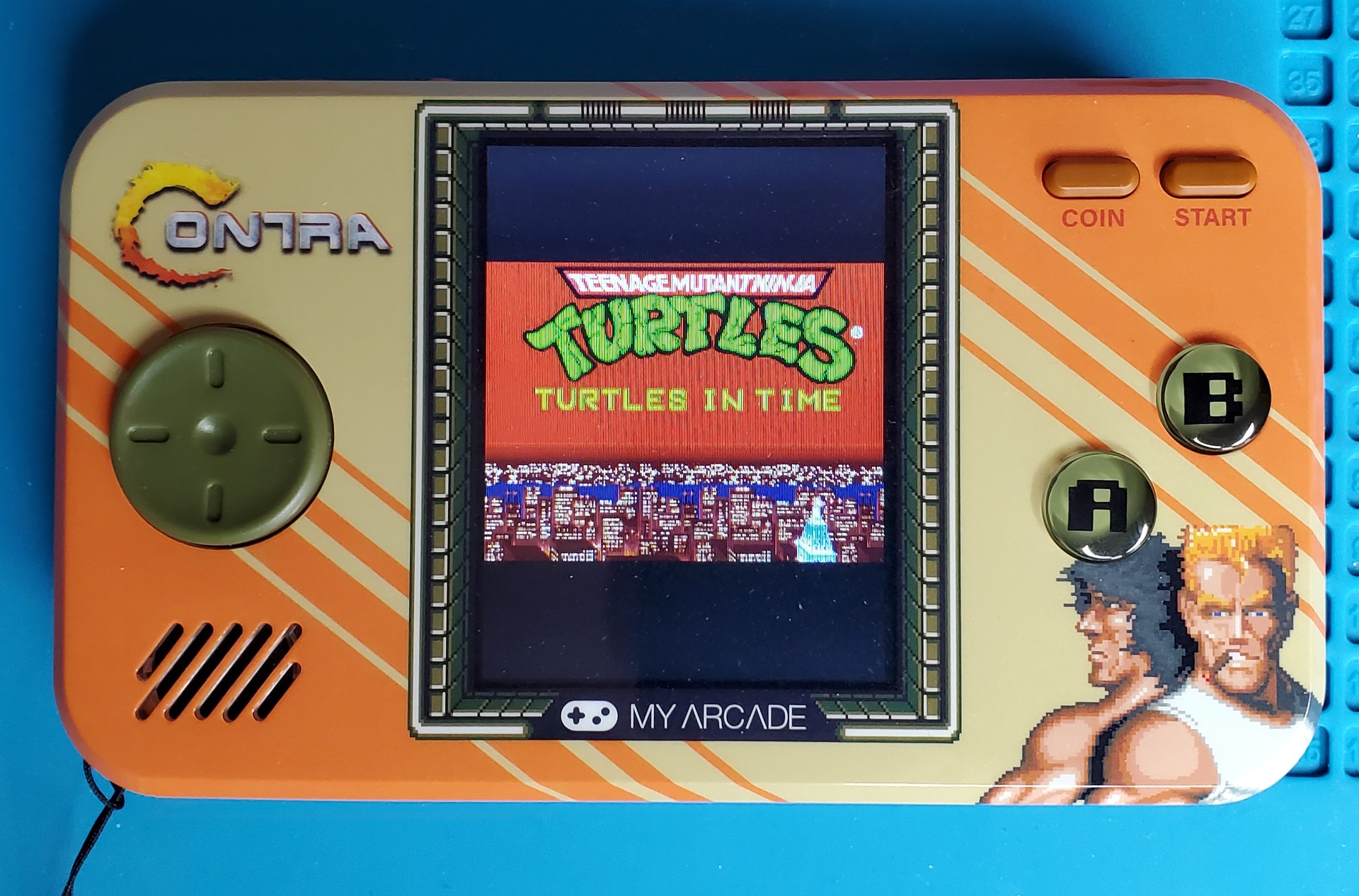
The other day I was walking through Target and noticed they had a bunch of collectable arcade systems available. They had everything from Pac-Man and Galaga to Contra. Some were full size standing cabinets (about 4 feet tall), while others were handheld versions. I picked up a few different handhelds to take a look at and most appeared to be your run-of-the-mill NES-on-a-chip Famiclone systems, which wouldn’t be super interesting for ROM swapping since they tend to have the games hard-coded onto the chip.

As I was looking over the options, this Contra handheld caught my attention for a few reasons. First, the box advertised a feature called “CO/VS Technology” which claims to allow two systems to connect together for multiplayer. Second, the system had a tall screen that more closely matched the proportions of the arcade version rather than the standard 4:3 that I would expect from a typical Famiclone. I ended up picking up a couple of the handhelds to take a closer look.

Teardown
Inside the game console, there are multiple components of interest.

The main SoC is a Rockchip RK3128, which is a quad-core Cortex-A7 with a Mali400 MP2 GPU. The system also has 2Gbit of DDR3 RAM and 1Gbit of storage via a Winbond serial NAND flash connected over an SPI interface. Additionally, there is a micro-USB port, an audio port, and a port for the CO/VS multiplayer connector.
Hardware Probing
My first attempt at getting data off of the system was to try and dump the flash. I hooked up my HydraBus (you could also use a Bus Pirate) and attempted to use flashrom to dump the data. Unfortunately, flashrom is typically used to operate on SPI NOR flash, but the Winbond W25N01GVZEIG is a NAND flash. So, we will need to read the NAND flash datasheet and write some commands manually.
After reviewing the block diagram from the datasheet, we learn the following:

- The flash is organized by blocks
- Blocks consist of 64 pages
- A page consists of 2,112 bytes of data
- 2,048 bytes of actual data
- 64 bytes reserved for ECC data
- A column address is used to index into the page to read specific bytes
To dump all of the data, we would need to load the first page, set our column address to 0, start reading data from the page, increment the column address, and repeat through all available pages.
Let’s check the pinout to see how we should hook this up to the HydraBus.

The SPI interface is fairly straightforward, so let’s go ahead and hook it up. I’m using PCBite probes here to avoid having to solder any wires to the chip.

To test our connection, let’s start with the Read JEDEC ID instruction. According to the datasheet, this will return 3 bytes that identify the manufacturer and device.

We need to send 0x9F followed by 8 dummy clocks and then read 3 bytes. Using the HydraBus, we can do this by entering into SPI mode and using the following command:
[ 0x9F 0x11 r:3 ]Let’s break down the command to see what we are doing here:
| Command | Description |
|---|---|
[ | Chip Select (CS) enable (active when pin is low) |
0x9F | Send the Read JEDEC ID command |
0x11 | Dummy byte to fill 8 clock cycles (can be any byte like 0x00) |
r:3 | Read the next 3 bytes sent from the NAND flash (this is our JEDEC ID) |
] | Chip Select (CS) disable (inactive when pin is high) |

We get back 0xEF 0xAA 0x21. Let’s compare this to what we expect from the datasheet.

We got the expected result, so we should be good to start dumping data.
Dumping the Flash….Maybe…
[ 0x03 0x00 0x00 0x00 r:255 ]Let’s break down the command again:
| Command | Description |
|---|---|
[ | Chip Select (CS) enable (active when pin is low) |
0x03 | Read the data command |
0x00 | Column Address CA[15:8] |
0x00 | Column Address CA[7:0] |
0x00 | Dummy byte to fill 8 clock cycles |
r:255 | Read the next 255 bytes sent from the NAND flash |
] | Chip Select (CS) disable (inactive when pin is high) |

At first glance, the data seems like it could be good, but after performing multiple reads from the same location, the data being returned was different every time. This meant that we would not be able to assemble an accurate dump of the flash.
I wasn’t sure if the issue was related to reading the NAND flash in-circuit or a configuration issue with the HydraBus. I considered breaking out a logic analyzer or oscilloscope to take a closer look, but before doing that, I found a much better way to get the data.
RTFM - USB Recovery
After doing some Google searching on the RK3128 SoC, I found that it is commonly used in Android devices and TV boxes. Looking into the Rockchip wiki, I found that many Rockchip devices support a USB recovery mode that can be triggered by holding the volume up key while powering on the device via USB.

Sure enough, powering on the device while holding the volume up button caused it to be detected as a RockUSB device in Mask ROM mode.

NAND Dump
Using rkflashtool, which speaks the RockUSB protocol, we can dump the NAND flash. The tool expects an offset and size in blocks of 512 bytes.
If we go back to the NAND datasheet, we can see that it contains 65,536 pages of data with 2,048 bytes per page for a total of 134,217,728 bytes of data. Dividing this by the 512 byte sector size gives us 262,144 total sectors. So, we can dump from sector 0 to 262,144.
sudo ./rkflashtool r 0 262144 > ~/Desktop/nand_dumps/nand_dump.binI recommend doing 1-2 additional dumps and comparing file hashes to ensure you got a good dump.

Our hashes match! Opening the dump in a hex editor, we can see a GUID Partition Table header.

Digging further into the dump, we can find a reference to the Contra ROM and what appears to be a MAME arcade emulator.

Part 2 Sneak Peek…
Stay tuned for Part II of this post, where we will dig into the NAND image, swap out the ROMs, and see what else we’re able to get running on this thing!
This post originally written for TrustedSec and posted here with permission.